Page 1 text
ECE 512 Project Paper, Spring 2026 1 Performance Benchmarking of NC-FETs Max Tobin, Quinn Mair, Andy Ko, Justin Wang Abstract The negative capacitance field-effect transistor (NC-FET) has emerged as a promising candidate for overcoming the fundamental subthreshold swing (SS) limit in conventional CMOS devices by leveraging ferroelectric-induced voltage amplification. This work analyzes the structure, operation, and performance of NC-FETs across a range of experimentally demonstrated and theoretically projected devices. Benchmarking shows that many devices achieve sub-60 mV/dec switching and improved electrostatic control compared to silicon FinFETs, with HfO 2-based ferroelectrics and gate-all-around (GAA) structures offering the most practical pathways forward. However, challenges such as switching delay, hysteresis, negative differential resistance (NDR), and CMOS integration at advanced nodes remain significant. Ongoing efforts in ferroelectric material engineering, capacitance matching, and device architecture optimization aim to address these limitations. Overall, NC-FETs demonstrate strong potential for next-generation low-power logic, though further advancements are required before widespread technological adoption can be realized. Introduction The negative capacitance field-effect transistor (NC-FET) has emerged as a promising device concept aimed at overcoming fundamental limitations in conventional transistor operation. By incorporating a ferroelectric material into the gate stack, NC-FETs exploit the phenomenon of negative capacitance to achieve internal voltage amplification. This allows the gate voltage to more effectively modulate the channel surface potential, enabling subthreshold swings (SS) below the conventional thermal limit of 60 mV/dec at room temperature. As a result, NC-FETs offer the potential to maintain high on-current (I ON) while operating at reduced supply voltages (V DD), making them attractive for low-power and energy- efficient logic applications. The motivation for NC-FETs arises from the growing challenges faced by traditional CMOS technologies as device dimensions continue to scale. In conventional MOSFETs, the subthreshold swing is fundamentally limited by thermionic carrier transport, which constrains how sharply a device can switch between the OFF and ON states. This limitation prevents further reductions in supply voltage without degrading performance, leading to increased power consumption and reduced efficiency in modern integrated circuits. As scaling progresses into the nanometer regime, these constraints have become a major bottleneck for continued improvements in both performance and energy efficiency. NC-FETs directly target this limitation by modifying the electrostatics of the gate stack rather than relying solely on geometric scaling. However, despite their strong theoretical advantages, experimental demonstrations of NC-FETs have shown significant variability across device structures, material systems, and fabrication approaches. Implementations range from planar silicon devices and FinFET geometries to transistors based on two-dimensional (2D) materials, often paired with ferroelectric layers such as HfO 2- based films, PZT, or ferroelectric polymers. While some devices report sub-60 mV/dec switching, other key metrics, including on-current, threshold voltage, and operating voltage, vary widely. Device Structure and Operation An NC-FET is structurally similar to a conventional MOSFET, except that a ferroelectric layer is incorporated into the gate stack together with the dielectric. In a standard MOSFET, the gate voltage controls
Page 2 text
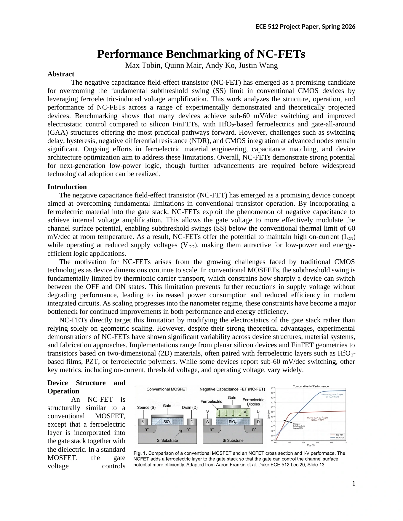
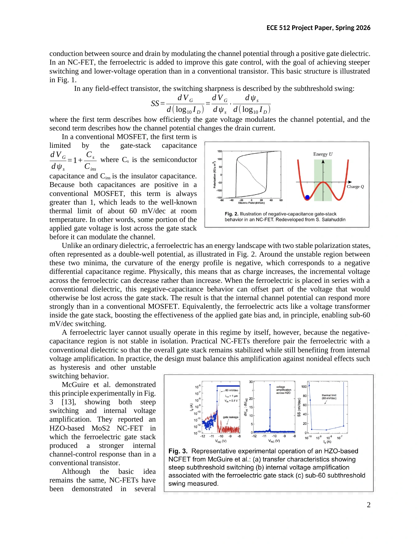
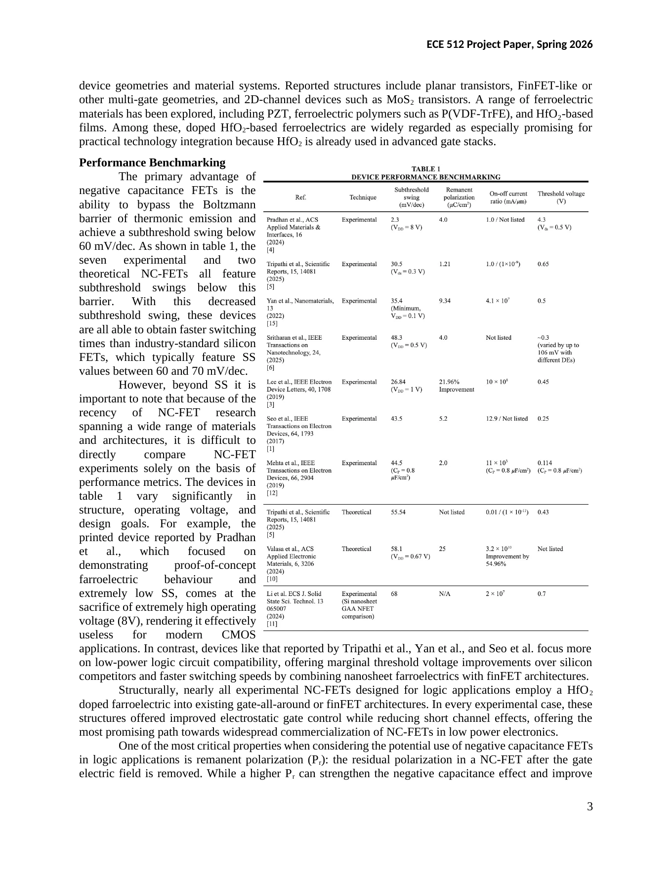
ECE 512 Project Paper, Spring 2026 2 conduction between source and drain by modulating the channel potential through a positive gate dielectric. In an NC-FET, the ferroelectric is added to improve this gate control, with the goal of achieving steeper switching and lower-voltage operation than in a conventional transistor. This basic structure is illustrated in Fig. 1. In any field-effect transistor, the switching sharpness is described by the subthreshold swing: SS = d V G d ( log10 I D ) = d V G d ψs ⋅ d ψs d ( log10 I D ) where the first term describes how efficiently the gate voltage modulates the channel potential, and the second term describes how the channel potential changes the drain current. In a conventional MOSFET, the first term is limited by the gate-stack capacitance d V G d ψs = 1 + Cs Cins where C s is the semiconductor capacitance and C ins is the insulator capacitance. Because both capacitances are positive in a conventional MOSFET, this term is always greater than 1, which leads to the well-known thermal limit of about 60 mV/dec at room temperature. In other words, some portion of the applied gate voltage is lost across the gate stack before it can modulate the channel. Unlike an ordinary dielectric, a ferroelectric has an energy landscape with two stable polarization states, often represented as a double-well potential, as illustrated in Fig. 2. Around the unstable region between these two minima, the curvature of the energy profile is negative, which corresponds to a negative differential capacitance regime. Physically, this means that as charge increases, the incremental voltage across the ferroelectric can decrease rather than increase. When the ferroelectric is placed in series with a conventional dielectric, this negative-capacitance behavior can offset part of the voltage that would otherwise be lost across the gate stack. The result is that the internal channel potential can respond more strongly than in a conventional MOSFET. Equivalently, the ferroelectric acts like a voltage transformer inside the gate stack, boosting the effectiveness of the applied gate bias and, in principle, enabling sub-60 mV/dec switching. A ferroelectric layer cannot usually operate in this regime by itself, however, because the negative- capacitance region is not stable in isolation. Practical NC-FETs therefore pair the ferroelectric with a conventional dielectric so that the overall gate stack remains stabilized while still benefiting from internal voltage amplification. In practice, the design must balance this amplification against nonideal effects such as hysteresis and other unstable switching behavior. McGuire et al. demonstrated this principle experimentally in Fig. 3 [13], showing both steep switching and internal voltage amplification. They reported an HZO-based MoS2 NC-FET in which the ferroelectric gate stack produced a stronger internal channel-control response than in a conventional transistor. Although the basic idea remains the same, NC-FETs have been demonstrated in several
Page 3 text
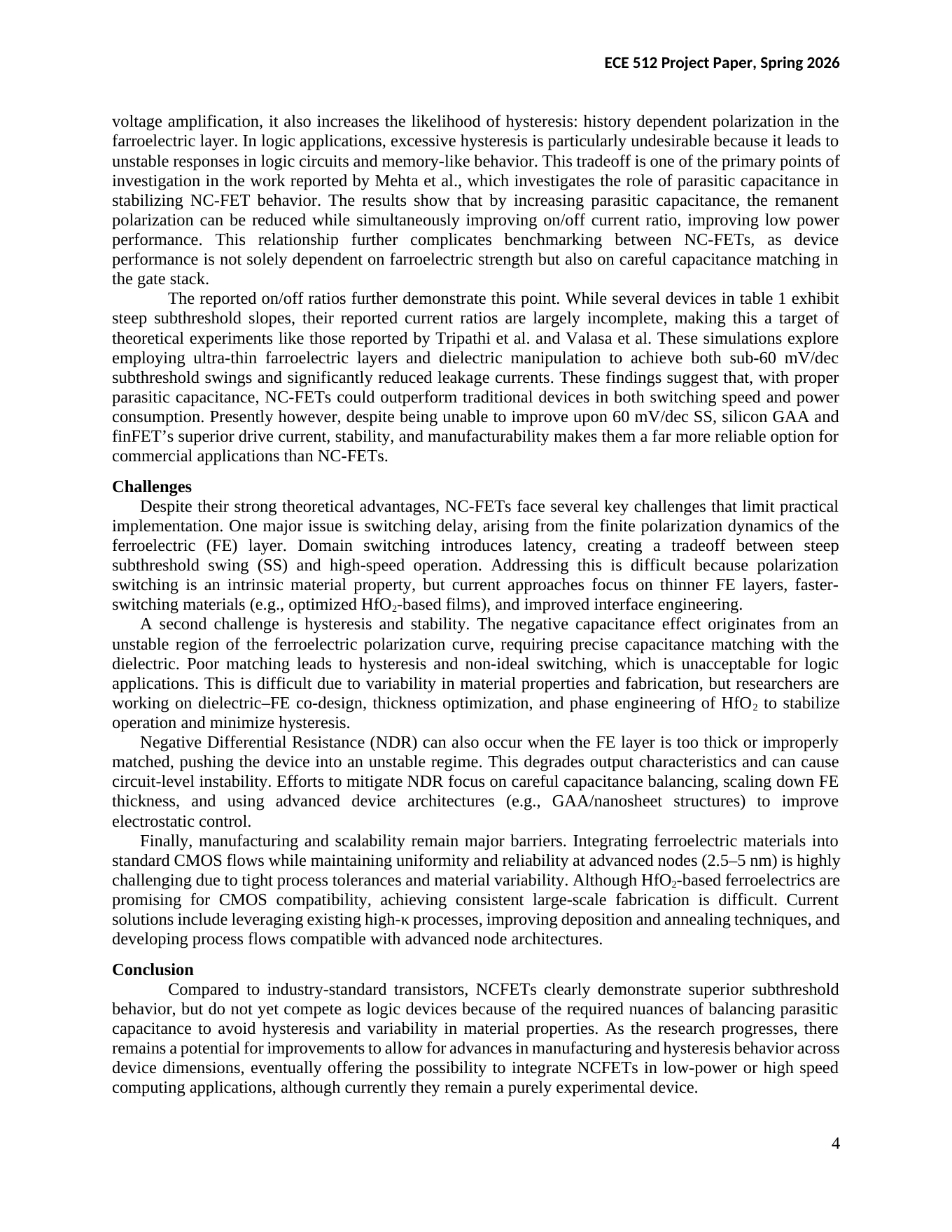
ECE 512 Project Paper, Spring 2026 3 device geometries and material systems. Reported structures include planar transistors, FinFET-like or other multi-gate geometries, and 2D-channel devices such as MoS 2 transistors. A range of ferroelectric materials has been explored, including PZT, ferroelectric polymers such as P(VDF-TrFE), and HfO₂-based films. Among these, doped HfO 2-based ferroelectrics are widely regarded as especially promising for practical technology integration because HfO2 is already used in advanced gate stacks. Performance Benchmarking The primary advantage of negative capacitance FETs is the ability to bypass the Boltzmann barrier of thermonic emission and achieve a subthreshold swing below 60 mV/dec. As shown in table 1, the seven experimental and two theoretical NC-FETs all feature subthreshold swings below this barrier. With this decreased subthreshold swing, these devices are all able to obtain faster switching times than industry-standard silicon FETs, which typically feature SS values between 60 and 70 mV/dec. However, beyond SS it is important to note that because of the recency of NC-FET research spanning a wide range of materials and architectures, it is difficult to directly compare NC-FET experiments solely on the basis of performance metrics. The devices in table 1 vary significantly in structure, operating voltage, and design goals. For example, the printed device reported by Pradhan et al., which focused on demonstrating proof-of-concept farroelectric behaviour and extremely low SS, comes at the sacrifice of extremely high operating voltage (8V), rendering it effectively useless for modern CMOS applications. In contrast, devices like that reported by Tripathi et al., Yan et al., and Seo et al. focus more on low-power logic circuit compatibility, offering marginal threshold voltage improvements over silicon competitors and faster switching speeds by combining nanosheet farroelectrics with finFET architectures. Structurally, nearly all experimental NC-FETs designed for logic applications employ a HfO 2 doped farroelectric into existing gate-all-around or finFET architectures. In every experimental case, these structures offered improved electrostatic gate control while reducing short channel effects, offering the most promising path towards widespread commercialization of NC-FETs in low power electronics. One of the most critical properties when considering the potential use of negative capacitance FETs in logic applications is remanent polarization (P r): the residual polarization in a NC-FET after the gate electric field is removed. While a higher P r can strengthen the negative capacitance effect and improve
Page 4 text
ECE 512 Project Paper, Spring 2026 4 voltage amplification, it also increases the likelihood of hysteresis: history dependent polarization in the farroelectric layer. In logic applications, excessive hysteresis is particularly undesirable because it leads to unstable responses in logic circuits and memory-like behavior. This tradeoff is one of the primary points of investigation in the work reported by Mehta et al., which investigates the role of parasitic capacitance in stabilizing NC-FET behavior. The results show that by increasing parasitic capacitance, the remanent polarization can be reduced while simultaneously improving on/off current ratio, improving low power performance. This relationship further complicates benchmarking between NC-FETs, as device performance is not solely dependent on farroelectric strength but also on careful capacitance matching in the gate stack. The reported on/off ratios further demonstrate this point. While several devices in table 1 exhibit steep subthreshold slopes, their reported current ratios are largely incomplete, making this a target of theoretical experiments like those reported by Tripathi et al. and Valasa et al. These simulations explore employing ultra-thin farroelectric layers and dielectric manipulation to achieve both sub-60 mV/dec subthreshold swings and significantly reduced leakage currents. These findings suggest that, with proper parasitic capacitance, NC-FETs could outperform traditional devices in both switching speed and power consumption. Presently however, despite being unable to improve upon 60 mV/dec SS, silicon GAA and finFET’s superior drive current, stability, and manufacturability makes them a far more reliable option for commercial applications than NC-FETs. Challenges Despite their strong theoretical advantages, NC-FETs face several key challenges that limit practical implementation. One major issue is switching delay, arising from the finite polarization dynamics of the ferroelectric (FE) layer. Domain switching introduces latency, creating a tradeoff between steep subthreshold swing (SS) and high-speed operation. Addressing this is difficult because polarization switching is an intrinsic material property, but current approaches focus on thinner FE layers, faster- switching materials (e.g., optimized HfO2-based films), and improved interface engineering. A second challenge is hysteresis and stability. The negative capacitance effect originates from an unstable region of the ferroelectric polarization curve, requiring precise capacitance matching with the dielectric. Poor matching leads to hysteresis and non-ideal switching, which is unacceptable for logic applications. This is difficult due to variability in material properties and fabrication, but researchers are working on dielectric–FE co-design, thickness optimization, and phase engineering of HfO 2 to stabilize operation and minimize hysteresis. Negative Differential Resistance (NDR) can also occur when the FE layer is too thick or improperly matched, pushing the device into an unstable regime. This degrades output characteristics and can cause circuit-level instability. Efforts to mitigate NDR focus on careful capacitance balancing, scaling down FE thickness, and using advanced device architectures (e.g., GAA/nanosheet structures) to improve electrostatic control. Finally, manufacturing and scalability remain major barriers. Integrating ferroelectric materials into standard CMOS flows while maintaining uniformity and reliability at advanced nodes (2.5–5 nm) is highly challenging due to tight process tolerances and material variability. Although HfO2-based ferroelectrics are promising for CMOS compatibility, achieving consistent large-scale fabrication is difficult. Current solutions include leveraging existing high-κ processes, improving deposition and annealing techniques, and developing process flows compatible with advanced node architectures. Conclusion Compared to industry-standard transistors, NCFETs clearly demonstrate superior subthreshold behavior, but do not yet compete as logic devices because of the required nuances of balancing parasitic capacitance to avoid hysteresis and variability in material properties. As the research progresses, there remains a potential for improvements to allow for advances in manufacturing and hysteresis behavior across device dimensions, eventually offering the possibility to integrate NCFETs in low-power or high speed computing applications, although currently they remain a purely experimental device.
Page 5 text
ECE 512 Project Paper, Spring 2026 5 References [1] J. Seo, J. Lee, and M. Shin, “Analysis of Drain-Induced Barrier Rising in Short-Channel Negative- Capacitance FETs and Its Applications,” IEEE Trans. Electron Devices, vol. 64, no. 4, pp. 1793– 1798, Apr. 2017, doi: 10.1109/TED.2017.2658673. [2] C.-H. Lin, B. Greene, H. Li, R. Kim, J. Kavalieros, and T. Ghani, “Beyond RibbonFET: Energy Efficiency Innovations to Drive Technology and Design for the Next Decade,” 2025. [3] S.-Y. Lee et al., “Experimental Demonstration of Stacked Gate- All-Around Poly-Si Nanowires Negative Capacitance FETs With Internal Gate Featuring Seed Layer and Free of Post-Metal Annealing Process,” IEEE Electron Device Lett., vol. 40, no. 11, pp. 1708–1711, Nov. 2019, doi: 10.1109/LED.2019.2940696. [4] J. R. Pradhan and S. Dasgupta, “Fully Printed Negative-Capacitance Field-Effect Transistors with Ultralow Subthreshold Swing and High Inverter Signal Gain,” ACS Appl. Mater. Interfaces, vol. 16, no. 30, pp. 39517–39527, Jul. 2024, doi: 10.1021/acsami.4c00548. [5] S. L. Tripathi, N. N. Prakash, B. Raj, and S. Hadiyoso, “High performance and low leakage heterojunction 10 nm PZT NC-FinFET for low power application,” Sci Rep, vol. 15, no. 1, p. 35891, Oct. 2025, doi: 10.1038/s41598-025-19866-y. [6] M. Sritharan, H. Lee, M. Spinazze, and Y. Yoon, “Implications of Dielectric Phases in Ferroelectric HfO$_{2}$ Films on the Performance of Negative Capacitance FETs,” IEEE Trans. Nanotechnology, vol. 24, pp. 67–72, 2025, doi: 10.1109/TNANO.2025.3531552. [7] E. Ko, J. W. Lee, and C. Shin, “Negative Capacitance FinFET With Sub-20-mV/decade Subthreshold Slope and Minimal Hysteresis of 0.48 V,” IEEE Electron Device Lett., vol. 38, no. 4, pp. 418–421, Apr. 2017, doi: 10.1109/LED.2017.2672967. [8] A. I. Khan et al., “Negative capacitance in a ferroelectric capacitor,” Nature Mater, vol. 14, no. 2, pp. 182–186, Feb. 2015, doi: 10.1038/nmat4148. [9] M. Hoffmann, S. Slesazeck, and T. Mikolajick, “Progress and future prospects of negative capacitance electronics: A materials perspective,” APL Materials, vol. 9, no. 2, p. 020902, Feb. 2021, doi: 10.1063/5.0032954. [10] S. Valasa, V. R. Kotha, and N. Vadthiya, “Pushing the Boundaries: Design and Simulation Approach of Negative Capacitance Nanosheet FETs with Ferroelectric and Dielectric Spacers at the Sub-3 nm Technology Node for Analog/RF/Mixed Signal Applications,” ACS Appl. Electron. Mater., vol. 6, no. 5, pp. 3206–3215, May 2024, doi: 10.1021/acsaelm.3c01862. [11] L. Li et al., “Stacked Si Nanosheets Gate-All-Around Transistors with Silicon-on-Nothing Structure for Suppressing Parasitic Effects and Improving Circuits’ Performance,” ECS J. Solid State Sci. Technol., vol. 13, no. 6, p. 065007, Jun. 2024, doi: 10.1149/2162-8777/ad5106. [12] H. Mehta and H. Kaur, “Study on Impact of Parasitic Capacitance on Performance of Graded Channel Negative Capacitance SOI FET at High Temperature,” IEEE Trans. Electron Devices, vol. 66, no. 7, pp. 2904–2909, Jul. 2019, doi: 10.1109/TED.2019.2917775. [13] K.-S. Li et al., “Sub-60mV-swing negative-capacitance FinFET without hysteresis,” in 2015 IEEE International Electron Devices Meeting (IEDM), Washington, DC, USA: IEEE, Dec. 2015, p. 22.6.1-22.6.4. doi: 10.1109/IEDM.2015.7409760. [14] F. A. McGuire et al., “Sustained Sub-60 mV/decade Switching via the Negative Capacitance Effect in MoS2 Transistors,” Nano Lett., vol. 17, no. 8, pp. 4801–4806, Aug. 2017, doi: 10.1021/acs.nanolett.7b01584. [15] S.-C. Yan, C.-H. Wu, C.-J. Sun, Y.-W. Lin, Y.-J. Yao, and Y.-C. Wu, “Trench FinFET Nanostructure with Advanced Ferroelectric Nanomaterial HfZrO2 for Sub-60-mV/Decade Subthreshold Slope for Low Power Application,” Nanomaterials, vol. 12, no. 13, p. 2165, Jun. 2022, doi: 10.3390/nano12132165. [16] S. Salahuddin and S. Datta, “Use of Negative Capacitance to Provide Voltage Amplification for Low Power Nanoscale Devices,” Nano Lett., vol. 8, no. 2, pp. 405–410, Feb. 2008, doi: 10.1021/nl071804g.
Page 6 text
ECE 512 Project Paper, Spring 2026 6 [17] X. Wang et al., “Van der Waals negative capacitance transistors,” Nat Commun, vol. 10, no. 1, p. 3037, Jul. 2019, doi: 10.1038/s41467-019-10738-4.